


- ADD: Room305, Building 1,17# GuangMing RD.Dongguan CityGuangdong China 523779
- TEL: +86 18681194949
- FAX: +86 0769-23380975
- Email: Support@inhaos.com


INHAOS Design Capability Introduction - PCB Layout
INHAOS have three professional PCB design engineers who have multinational companies' working experience and rich practical experience. INHAOS design and develop all products by its own engineers. We can also customize for customers’ require.
Our design experience involve in Single-layer to 8-layer, mixed analog and digital design. The maximum operating frequency can reach 3.2GHz. The largest NET is more than 65000. Nowadays, these products are stably running in everywhere of the world.
Our biggest advantage is our designed can fully meet mass production manufacturing. Even though for engineering validation sample, we also use thorough DFM (Design For Manufacture) process to handle. Thanks for our engineers’ rich product design experience and PCB manufacturer’s support, we consider sample debugging, assembly, automatically testing at the initial stage of PCB designing. Customers can directly submit circuit diagram to us, then we give the design which have been confirmed by customers to our PCB partners for producing. We can even directly assemble and debug samples for customers. All depends on customers’ requirements.
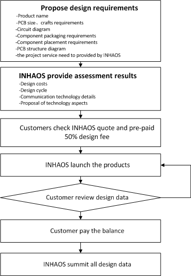
Our PCB design cooperation process shows below:
Some of our design projects show below:
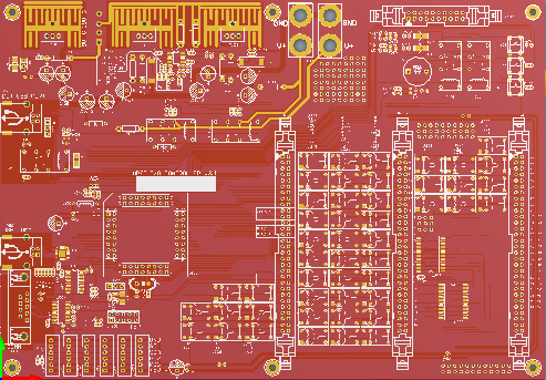
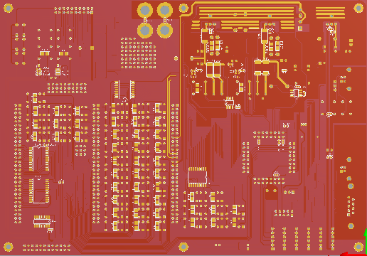
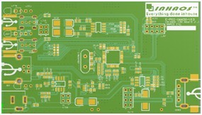
Project 1: Industrial data acquisition and control system, 6 Layer,230*160mm. Total parts is 308, total network is 1412. Main design features: fully considering industrial environment’s anti-interference and stability.
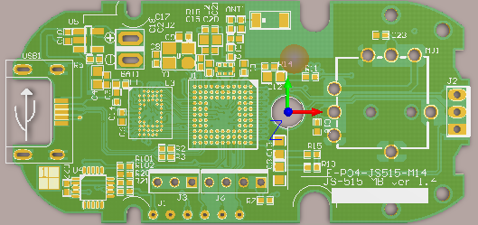
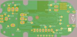
Project 2: Bluetooth game controller, 4 layer,53*25mm, total parts is 53, total network is 95.
Main design features: Micro BGA chipset, Fully coordinate with complicated ME design and meet the standard of EMI test in limited space. It requires putting the test point in non-interference ME position for the convenience of mass production.
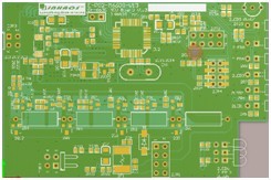
Project 3: USB current measurement Hub, two double -side PCB, total parts is 202, network is 265.
Main design features: Double-side panel design crafts meet the strict requirements of USB 2.0 High speed (480Mbps)and also meet the current measurement of 0.5uA resolution. The test results prove PCB design is reliable, can meet all kinds of design’s requirement.
We still have a lot of design cases not mentioned here. If you have design requirement, please feel free to contact us.
Copyright © 2010 INHAOS Technology Co., Limited. All Rights Reserved. (Ver 1.0.0000)Powered by Onepound